← 500W Mosfet Power Inverter Schematic: Build Your Own High-Power Inverter! 500w mosfet inverter circuit diagram sine inverter circuit m Arduino Nano Footprint & Symbol: Essential Guide for PCB Designers! How to connect & blink an led with arduino →
If you are looking for Collaboration for Mechanical & PCB Designers | Guides | Altium 365 you've came to the right web. We have 25 Images about Collaboration for Mechanical & PCB Designers | Guides | Altium 365 like High Speed Layout Design Guidelines | PDF | Capacitor | Printed Circuit, PCB Trace Basics For PCB Designers | Reversepcb and also PCB Layers: Everything You Need to Know. Here it is:
Collaboration For Mechanical & PCB Designers | Guides | Altium 365
 resources.altium365.com
Collaboration for Mechanical & PCB Designers | Guides | Altium 365
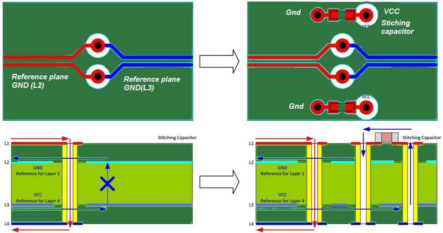
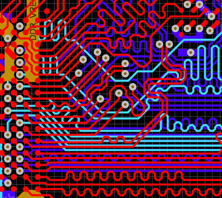
Ddr Pcb Layout Guidelines
 learningschoolunavowed.z14.web.core.windows.net
Ddr Pcb Layout Guidelines
Guide To PCB Trace Length Matching In High Speed Design | NWES Blog
 www.nwengineeringllc.com
Guide to PCB Trace Length Matching in High Speed Design | NWES Blog
11 Best High-Speed PCB Routing Practices – PCB HERO
 www.pcb-hero.com
11 Best High-Speed PCB Routing Practices – PCB HERO
PCB Standards: An Engineer's Guide
 www.ultralibrarian.com
PCB Standards: An Engineer's Guide
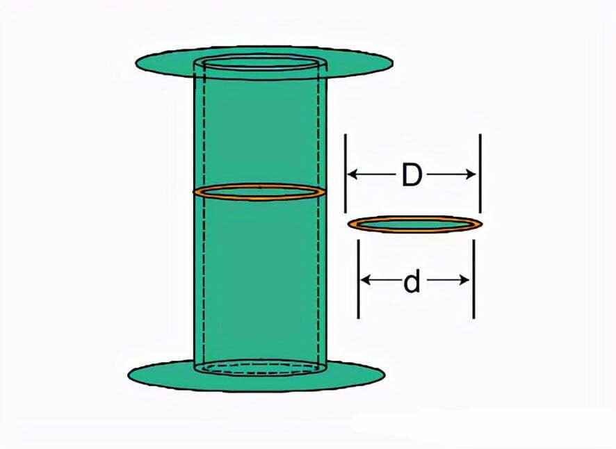
Demystifying Standard FR4 Thickness: A Comprehensive Guide For PCB
 ksnpcb.com
Demystifying Standard FR4 Thickness: A Comprehensive Guide for PCB ...
High-Speed PCB Layout: Physical Design Issues Of High-Speed Interfaces
 www.mentor.com
High-Speed PCB Layout: Physical Design Issues of High-Speed Interfaces ...
Optimizing PCB Cleanliness Testing | Techspray
 www.techspray.com
Optimizing PCB Cleanliness Testing | Techspray
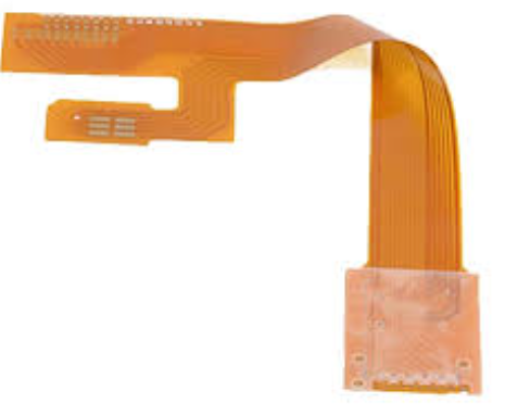
Qualcomm Snapdragon APQ8016 Fanout
 fedevel.com
Qualcomm Snapdragon APQ8016 fanout
PCB Layout Guidelines For High Speed Applications - HardwareBee
 hardwarebee.com
PCB Layout Guidelines For High Speed Applications - HardwareBee
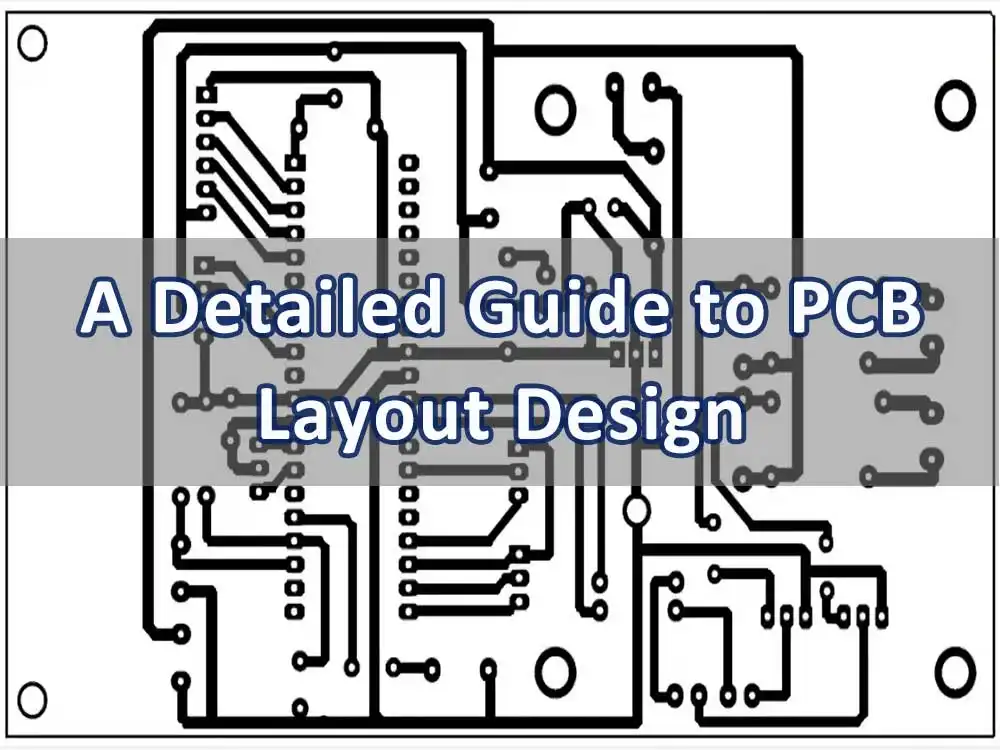
Complete Guide To PCB Layout Design Steps And Rules Circuit Diagram
 declanstarling.pages.dev
Complete Guide To PCB Layout Design Steps And Rules Circuit Diagram ...
High Speed Pcb Design And Layout, Expert PCB Design Service [ With Step
 www.venture-mfg.com
High Speed Pcb Design and Layout, Expert PCB Design Service [ With Step ...
Ultimate Guide To Emc Pcb Design And Emc Standards 20 | XXX Porn Sex Pics
 www.hotzsexywomen.com
Ultimate Guide To Emc Pcb Design And Emc Standards 20 | XXX Porn Sex Pics
Qualcomm Snapdragon APQ8016 Fanout
 fedevel.com
Qualcomm Snapdragon APQ8016 fanout
Effects Of High-Speed Signals In PCB Design | Sierra Circuits
 www.protoexpress.com
Effects of High-Speed Signals in PCB Design | Sierra Circuits
Advanced Pcb Layout Includes High Speed Layout - Andwin Circuits
 www.andwinpcb.com
Advanced pcb layout includes high speed layout - Andwin Circuits
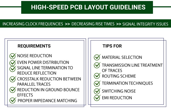
High Speed Layout Design Guidelines | PDF | Capacitor | Printed Circuit
 www.scribd.com
High Speed Layout Design Guidelines | PDF | Capacitor | Printed Circuit ...
Decoding PCB Design Cost: A Comprehensive Guide - AnyPCBA
 www.anypcba.com
Decoding PCB Design Cost: A Comprehensive Guide - AnyPCBA
PCB Trace Basics For PCB Designers | Reversepcb
 reversepcb.com
PCB Trace Basics For PCB Designers | Reversepcb
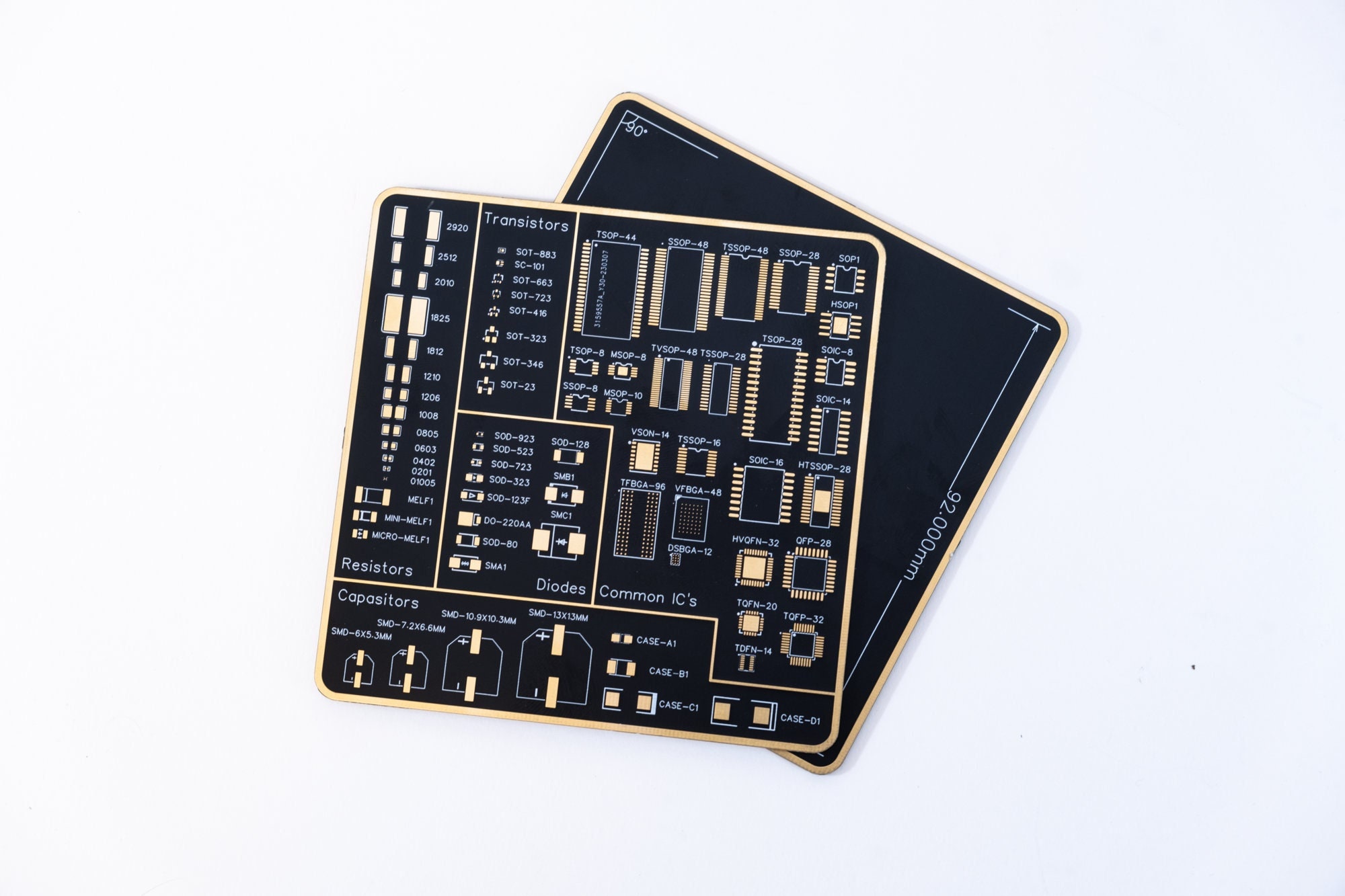
PCB Coasters For Designers PCB Footprint Guide - Etsy
 www.etsy.com
PCB Coasters for Designers PCB Footprint Guide - Etsy
Main Design Guidelines & Layout Rules On High Speed PCB
 www.integrasources.com
Main Design Guidelines & Layout Rules on High Speed PCB
An Ultimate Guide To PCB Wiring And Layout
 hillmancurtis.com
An Ultimate Guide To PCB Wiring And Layout
PCB Layers: Everything You Need To Know
 www.mktpcb.com
PCB Layers: Everything You Need to Know
[PDF] Intro To PCB Design: A Beginner’s Guide To Mastering PCB Layout
![[PDF] Intro to PCB Design: A Beginner’s Guide to Mastering PCB Layout](https://www.raypcb.com/wp-content/uploads/2023/02/PCB-Design-Guidelines-For-EMI-EMC.jpg) wiringtoolsreview.blogspot.com
wiringtoolsreview.blogspot.com
[PDF] Intro to PCB Design: A Beginner’s Guide to Mastering PCB Layout ...
PCB Panelization: A Comprehensive Technical Guide For PCB Designers
 www.mktpcb.com
PCB Panelization: A Comprehensive Technical Guide for PCB Designers
Pcb standards: an engineer's guide. Ddr pcb layout guidelines. Main design guidelines & layout rules on high speed pcb