← DIY Powerhouse: Build a 1000W Pure Sine Wave Inverter with EGS002 – Step-by-Step Guide! Diy photography projects: 10 easy builds you can start today Extra Large Subwoofer Amplifier: Huge 32-Inch Powerhouse! Bryston, 2b sst, solid state power amplifier →
If you are searching about PCB Design & Layout - PCB Design & Engineering Services you've came to the right web. We have 25 Pics about PCB Design & Layout - PCB Design & Engineering Services like High-Speed PCB Design Guidelines, Tips And PCB Design Guidelines For EMI And EMC Sierra Circuits and also Spotting DDR4 Impedance Violations in High Speed PCB Design | Blogs. Here you go:
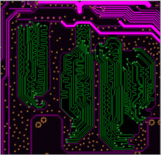
PCB Design & Layout - PCB Design & Engineering Services
 www.freedomcad.com
PCB Design & Layout - PCB Design & Engineering Services
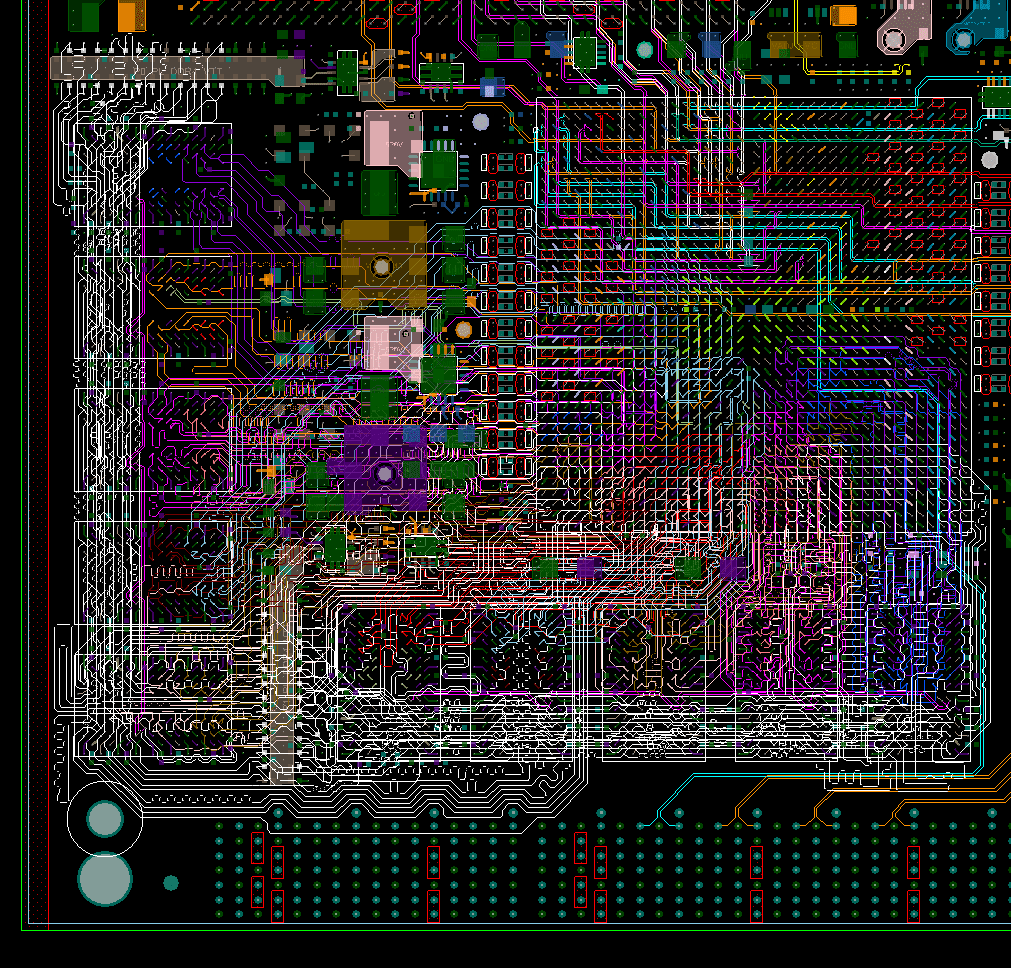
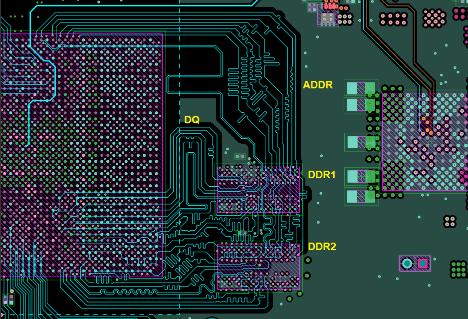
Migrating Your Embedded PCB Design From DDR2/3 To DDR4 SDRAMs
 www.embedded.com
Migrating your embedded PCB design from DDR2/3 to DDR4 SDRAMs ...
RF PCB Design: A Practical Guide For Engineers | Viasion
 www.viasion.com
RF PCB Design: A Practical Guide for Engineers | Viasion
PCB Design For Low-EMI DC/DC Converters - EDN Asia
 www.ednasia.com
PCB design for low-EMI DC/DC converters - EDN Asia
High Speed Pcb Design And Layout, Expert PCB Design Service [ With Step
 www.venture-mfg.com
High Speed Pcb Design and Layout, Expert PCB Design Service [ With Step ...
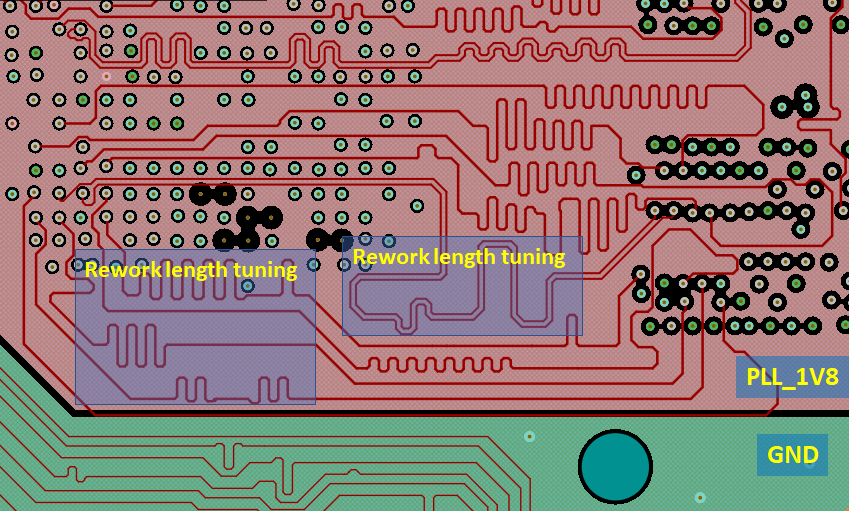
Spotting DDR4 Impedance Violations In High Speed PCB Design | Blogs
 resources.altium.com
Spotting DDR4 Impedance Violations in High Speed PCB Design | Blogs ...
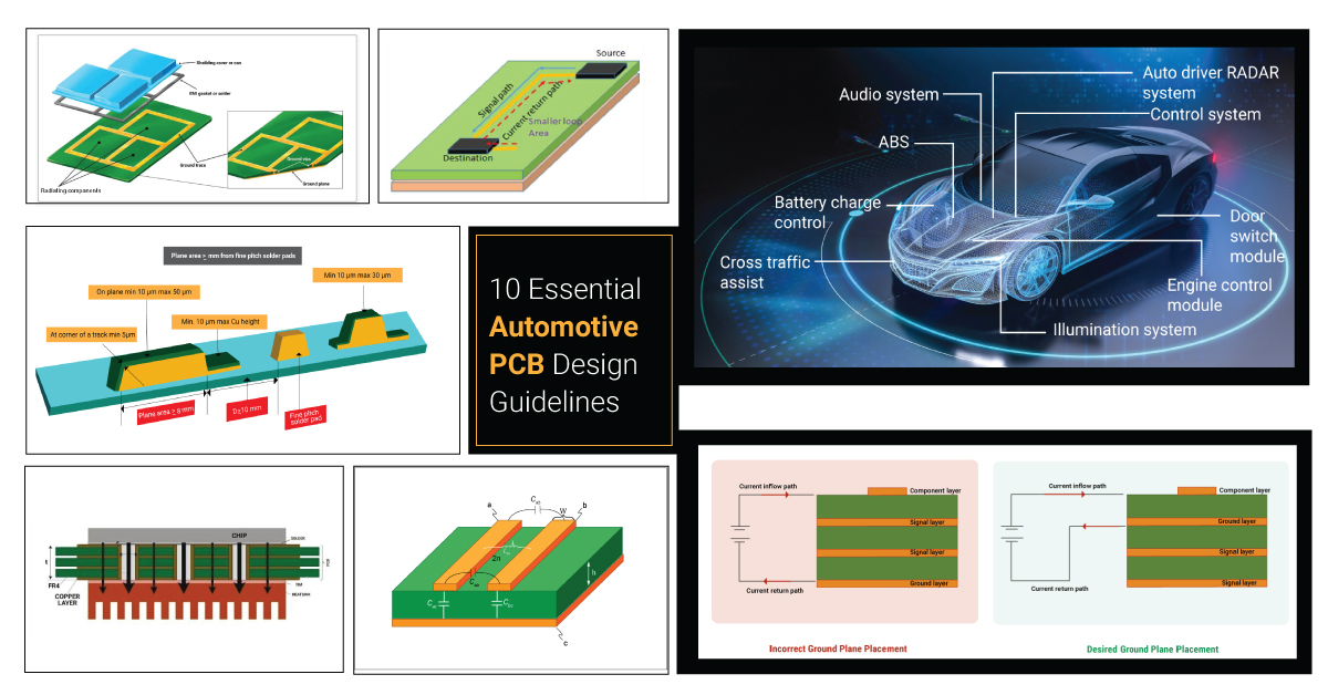
10 Automotive PCB Design Guidelines | Sierra Circuits
 www.protoexpress.com
10 Automotive PCB Design Guidelines | Sierra Circuits
18 PCB Layout Tips For Improving Your PCB Design And Reducing
 camptechii.com
18 PCB Layout Tips for Improving Your PCB Design and Reducing ...
Tips And PCB Design Guidelines For EMI And EMC Sierra Circuits
 www.designinte.com
Tips And PCB Design Guidelines For EMI And EMC Sierra Circuits ...
PCB Schematic And Layout: A Comprehensive Guide – Hillman Curtis
 hillmancurtis.com
PCB Schematic and Layout: A Comprehensive Guide – Hillman Curtis ...
11 Best High-Speed PCB Routing Practices – PCB HERO
 www.pcb-hero.com
11 Best High-Speed PCB Routing Practices – PCB HERO
How To Design A High Current PCB - RayPCB
 www.raypcb.com
How To Design A High Current PCB - RayPCB
DDR4 PCB Layout: Best Practices For Optimal Performance – Hillman
 hillmancurtis.com
DDR4 PCB Layout: Best Practices for Optimal Performance – Hillman ...
Pcb Routing Guidelines - Design Talk
 design.udlvirtual.edu.pe
Pcb Routing Guidelines - Design Talk
PCB Layout Guidelines And Considerations
 www.microcontrollertips.com
PCB layout guidelines and considerations
11 Best High-Speed PCB Routing Practices | Sierra Circuits
 www.protoexpress.com
11 Best High-Speed PCB Routing Practices | Sierra Circuits
LPDDR4 PCB Layout Guidelines | Zuken EN
 www.zuken.com
LPDDR4 PCB Layout Guidelines | Zuken EN
Inspirasi Pcb Routing, Skema Pcb
 skemadriver.blogspot.com
Inspirasi Pcb Routing, Skema Pcb
High-Speed PCB Design Guidelines
 circuits-diy.com
High-Speed PCB Design Guidelines
High Speed Pcb Layout Guidelines - Design Talk
 design.udlvirtual.edu.pe
High Speed Pcb Layout Guidelines - Design Talk
Layout Automation And Simulation Reap The Benefits Of DDR4
 www.techdesignforums.com
Layout automation and simulation reap the benefits of DDR4
Spotting DDR4 Impedance Violations In High Speed PCB Design | Blogs
 resources.altium.com
Spotting DDR4 Impedance Violations in High Speed PCB Design | Blogs ...
PCB Design Rules And Tips
 www.6pcb.com
PCB Design Rules and Tips
DDR4 PCB Design With ENIG Surface Finish And 6mil Minimum Trace Width
 www.hascendpcb.com
DDR4 PCB Design with ENIG Surface Finish and 6mil Minimum Trace Width ...
Nine Dot Connects » Altium Designer PCB Editor, Nine Dot Connects, 9dot
 www.ninedotconnects.com
Nine Dot Connects » Altium Designer PCB Editor, Nine Dot Connects, 9dot ...
Tips and pcb design guidelines for emi and emc sierra circuits. Rf pcb design: a practical guide for engineers. pcb design for low-emi dc/dc converters